


")


40px
80px
80px
80px
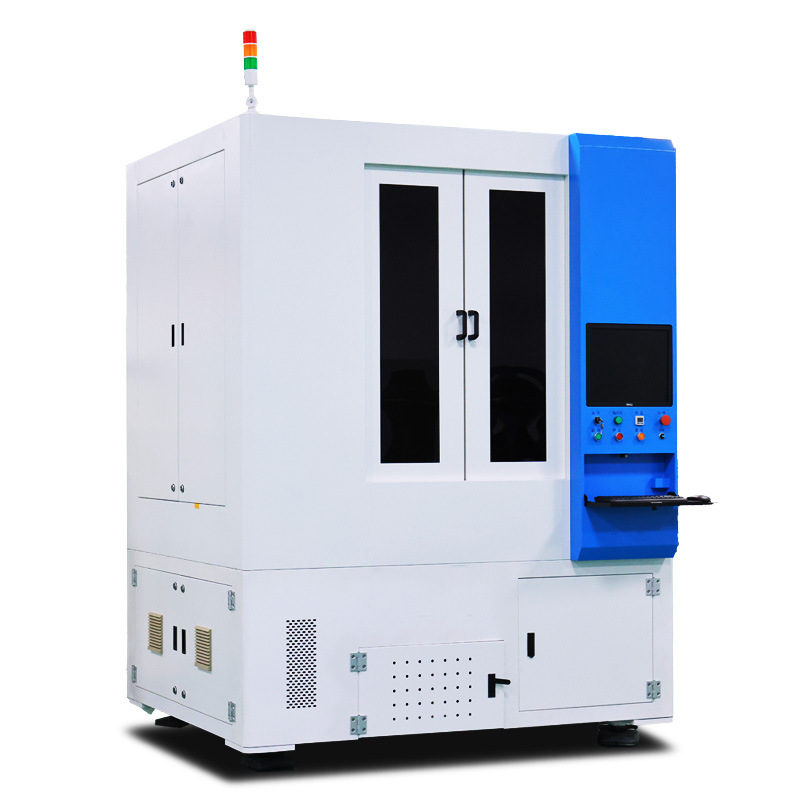
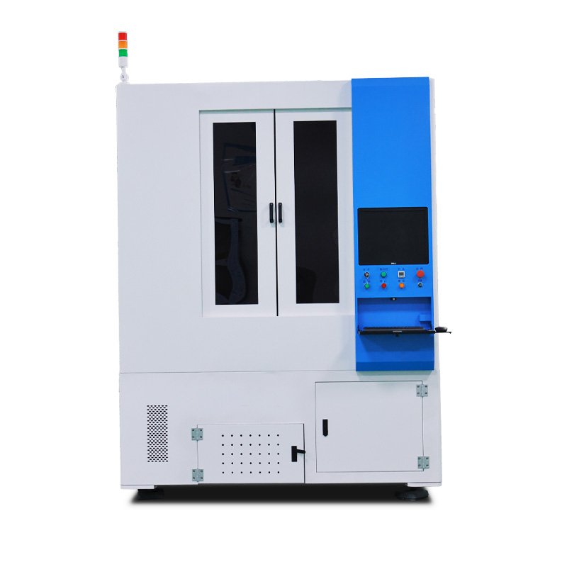
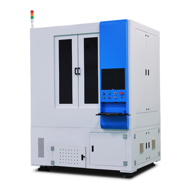
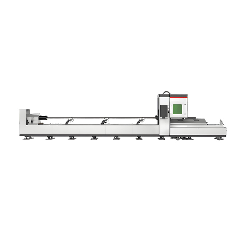
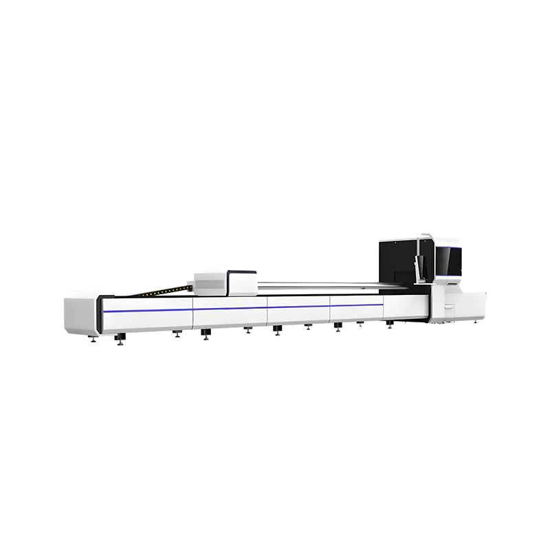
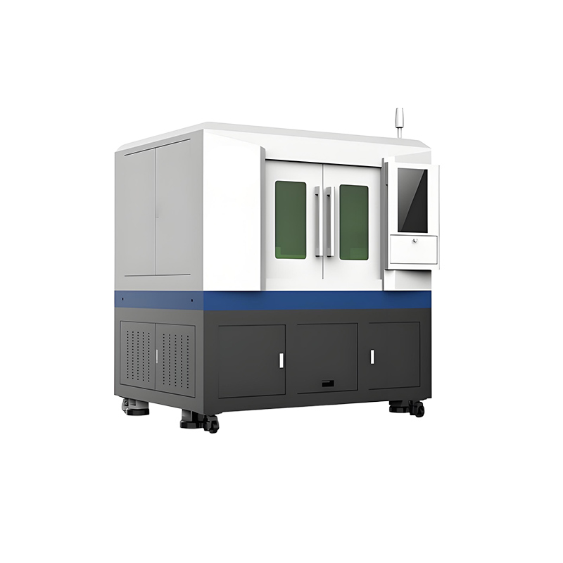
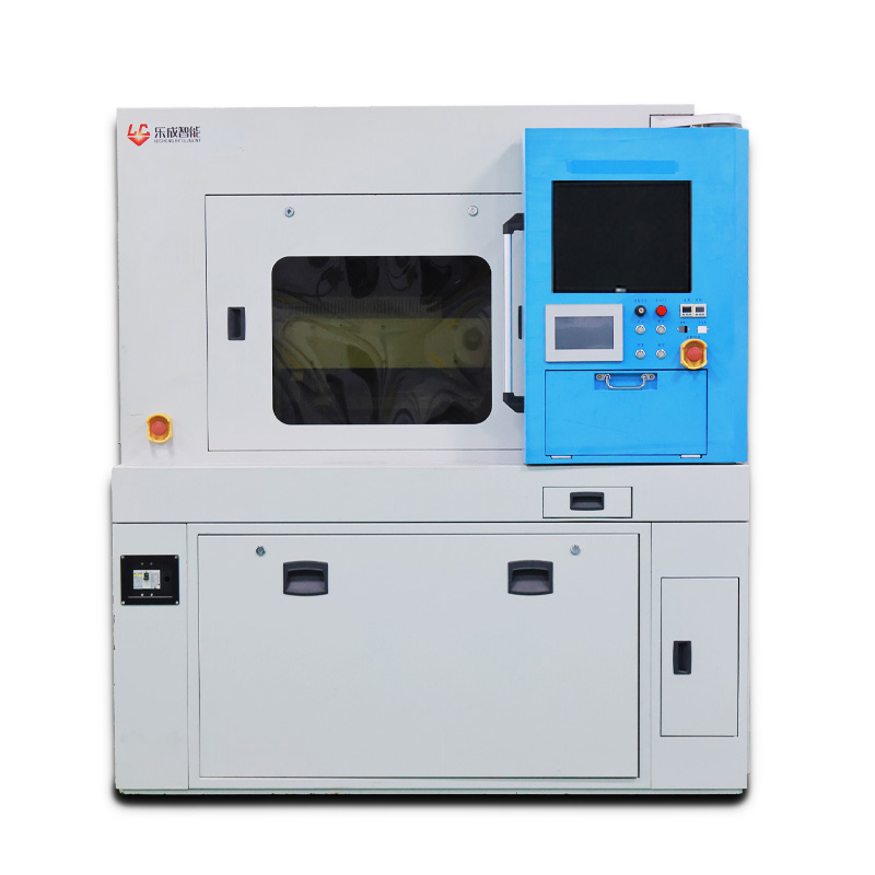
Laser Etching Equipment is designed for industrial laser processing projects that require stable beam control, process repeatability, and reliable integration with production requirements. For ├ Laser Cutting Equipment selection, buyers should compare material type, processing accuracy, automation level, throughput, maintenance access, and after-sales support before confirming the final equipment configuration.
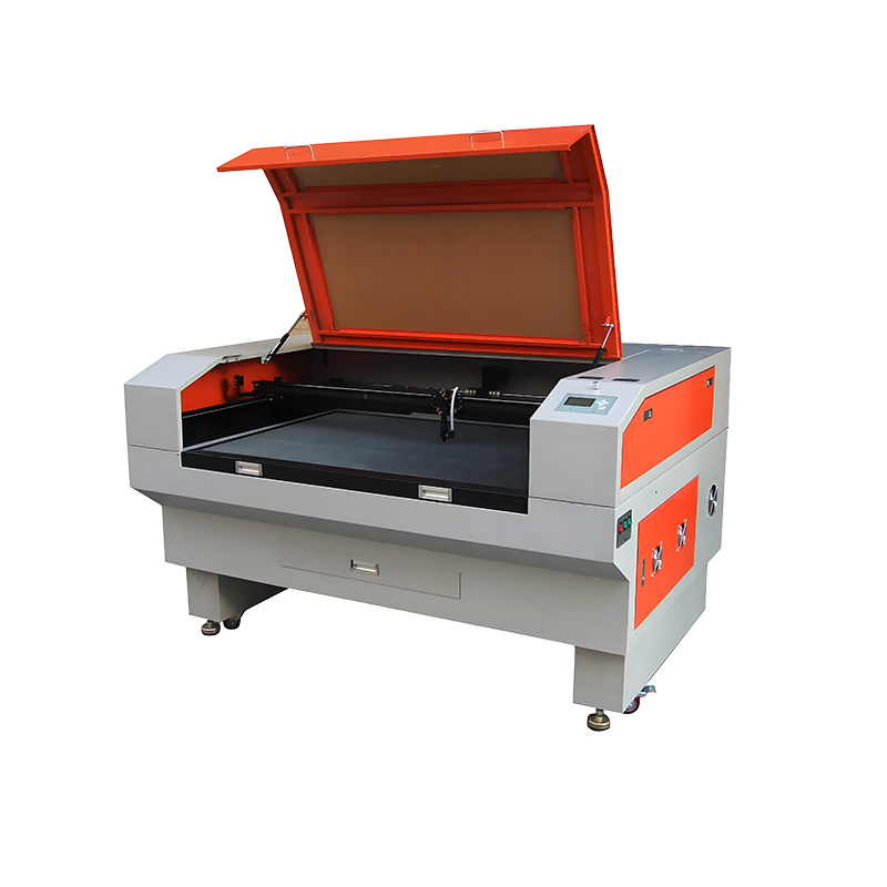
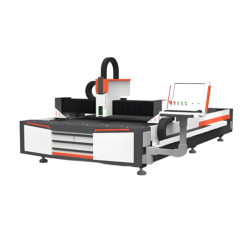
Related laser solutions include Laser High Precision Micro Machining Equipment, Fiber laser cutter, Desktop metal laser cutter. These internal references help users compare similar systems and move naturally between cleaning, cutting, scribing, marking, welding, and photovoltaic laser equipment pages.
Our laser etching system integrates cutting-edge engineering for unparalleled performance:
Ultra-Stable Laser Source: Fiber/UV/Picosecond lasers with adjustable pulse duration (ns/ps/fs), wavelength options (355nm, 532nm, 1064nm), and peak power up to 50W.
High-Precision Motion System: Air-bearing granite stage with ±1μm positioning accuracy, coupled with galvanometer scanning (7mm²–300mm² FOV) for dynamic patterning.
Intelligent Control Suite:
Real-time Z-axis autofocus (resolution: 0.1μm)
CCD vision alignment for ±5μm overlay accuracy
HMI with proprietary software supporting DXF, Gerber, BMP formats
Multi-Layer Environmental Control:
Class 1000 cleanroom-compatible enclosure
Active temperature-humidity regulation (±0.5°C)
Integrated fume extraction with HEPA filtration
Modular Upgrade Path: Optional 3-axis rotary stage, in-situ profilometry, or multi-laser hybrid configuration.

Revolutionize your manufacturing with core technological edges:
Sub-Micron Precision: Achieve 5–20μm feature sizes (Ra < 0.2μm) through diffraction-limited beam shaping.
Zero-Contact Processing: Eliminate tool wear and mechanical stress for brittle materials (e.g., SiC, glass).
Adaptive Energy Control: Pulse-by-pulse power modulation (1–100% in 0.1% steps) enables selective ablation of multilayers (e.g., ITO/Ag/PET).
Speed & Efficiency: 2000 mm/s scan speed with 50g acceleration; 4x faster than chemical etching.
Eco-Conscious Operation: 30% lower energy consumption vs. competitors; no toxic etchants or wastewater.

Empowering innovation across industries:
| Sector | Use Cases | Key Benefits |
|---|---|---|
| Semiconductors | Wafer dicing, IC trimming, package marking | <10μm kerf width, zero micro-cracks |
| FPD/LED | FPC patterning, OLED encapsulation removal, touch sensor etching | Selective ablation, 99.9% yield rate |
| Solar | PERC cell drilling (10–20μm holes), thin-film scribing | 500 holes/sec, ±2μm positional accuracy |
| Medical Devices | Stent texturing, implant micro-grooving, lab-on-chip channel fabrication | Biocompatible surface modification |
| Advanced R&D | 2D material processing, metasurface creation, quantum device prototyping | Nanosecond thermal im |
40px
80px
80px
80px